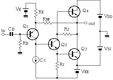
Envision the circuit of the SIT power amplifier
Circuit plan 1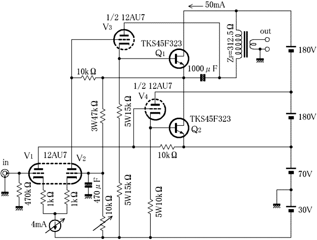
Tamura's PP transformer F-781 can be connected in parallel because two windings of 2.5 kΩ on the primary side are independently drawn out to the terminals, and when connected in parallel, the impedance becomes 1/4 of 625 ohms.
When 8Ω is loaded on the 16Ω terminal on the secondary side, the primary side becomes 312.5Ω, so I tried to draw a load line with this.
In the gate-drain voltage 450V at maximum rating of SIT, the gate-source voltage is generally a 20V, V D -I D towards the characteristic graph V D because it is documented = 600V, equivalent of a voltage It may be strong.
However, since it is an expensive element, I will avoid using it unreasonably.
If the operating point is V D = 180V, I D = 50mA and the load line of 312.5Ω is drawn , V D = 13V, I D = 584mA, and the maximum output is 44.6W at V GS = 0V .
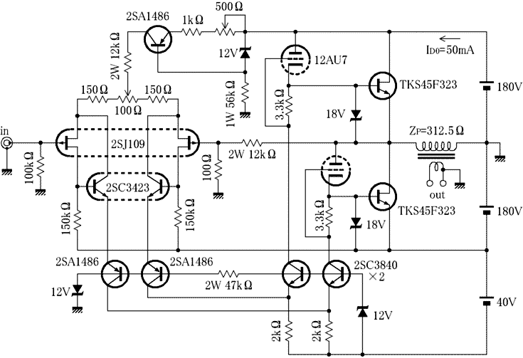
The circuit is a hybrid system that assists SIT with a vacuum tube.
In order to prevent a large current from flowing through the SIT when the balance is lost, a capacitor is inserted in the output to cut DC.
The SIT is driven by the cathode follower of V3 and V4.
Even when Q1 and Q2 are fully swung by the DC voltage level shift between the cathode grid of V3 and V4, the first stage differential circuit of V1 and V2 can be prevented from being cut off. This method mimics what the Yamaha B-1 was doing with the SIT.
Since only the DC voltage component of the output point is fed back to the first stage differential circuit, it seems that there is no feedback to the audio component at first glance, but NFB is applied to the cathode of V1 via the plate internal resistance of V2.
Since the internal resistance of the SIT is about 130Ω at this operating point, the damping factor is about 5 even if there is no feedback, so I
thought that it would be practical enough if NFB acts on this. However, there seems to be no room for open-loop gain, so I can't tell without experimenting.
Since the output transformer carries V3 plate current, it must be able to withstand DC superimposition.
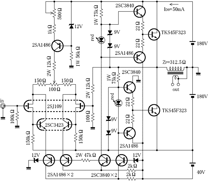
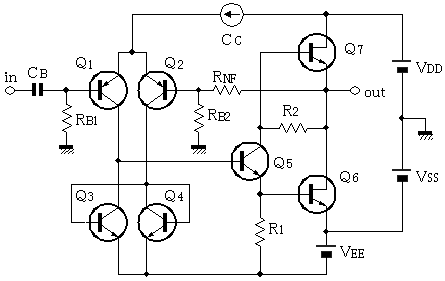
Circuit plan 2
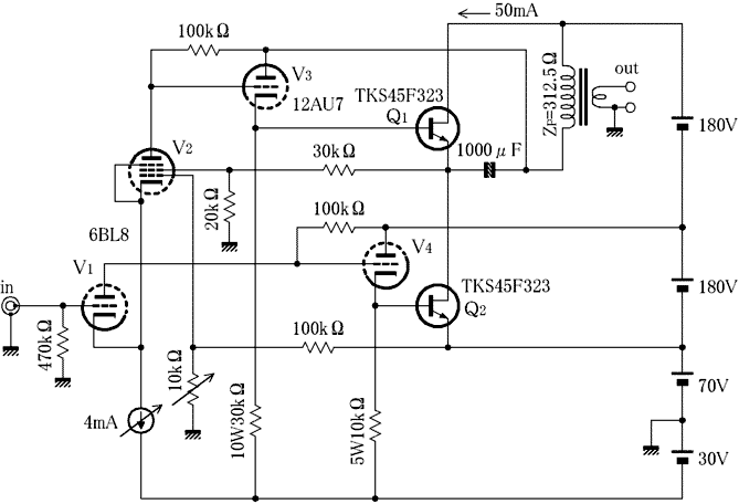
Multiply G2 of V2 by NFB
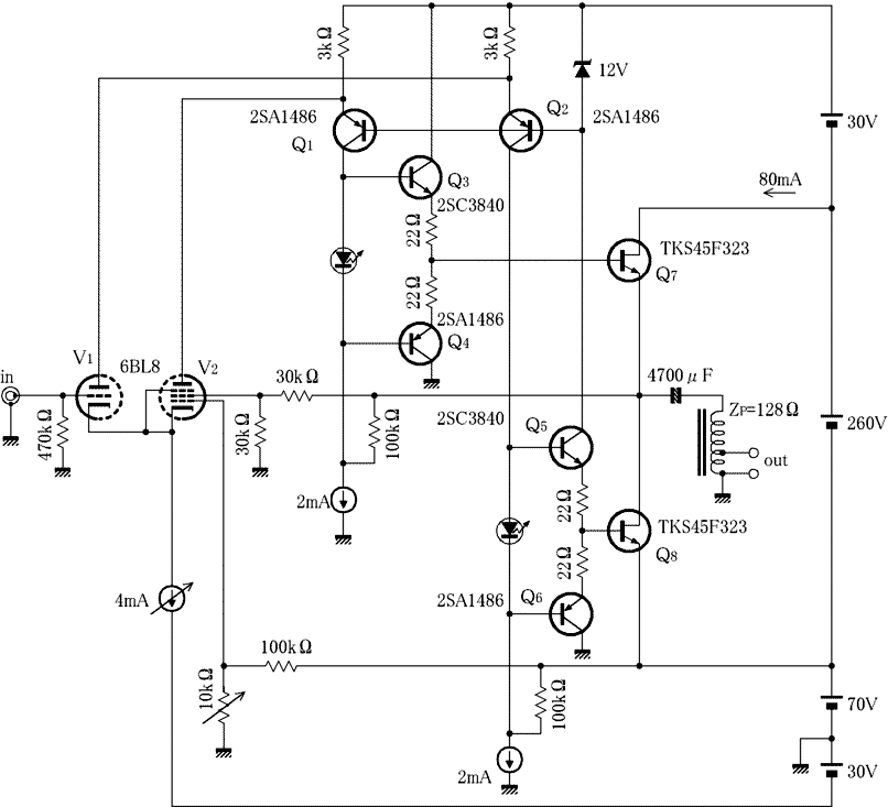
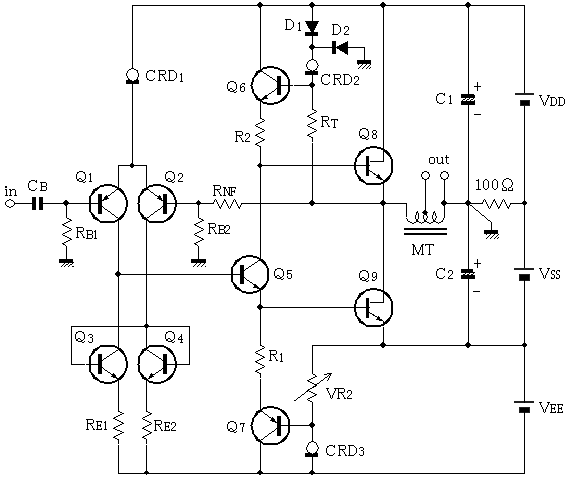
Circuit plan 3
Circuit plan 4
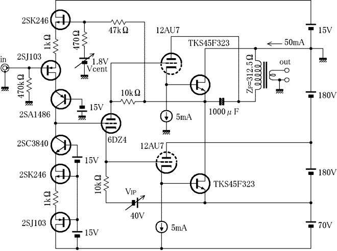
Uses PK phase inversion by 6DZ4. In the first stage, active load increases the gain and makes NFB effective.
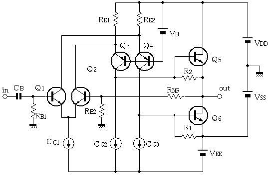
Circuit plan 5
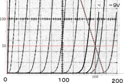
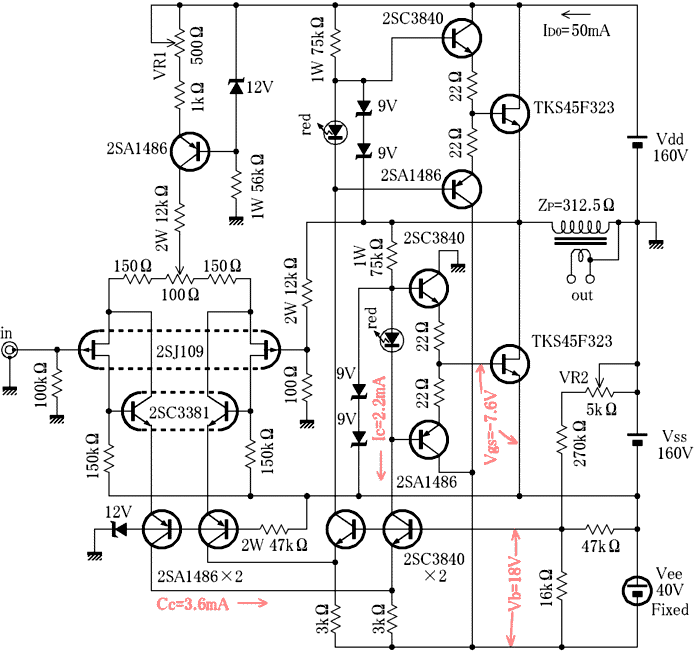
Reading the three constants at the operating point (VDS = 160V, ID = 50mA) of the
TK45F323 from the characteristic diagram, it is approximately μ = 23, gm = 0.18S, rp = 133Ω.
When 100% DG feedback is applied to TK45F323, the output resistance becomes 2.7Ω, so negative feedback of the overall is not necessary, but in order to keep the DC voltage at the neutral point stable, negative feedback is also applied to the overall.
The first stage improves linearity with an inverted Darlington connection.
Circuit plan 6
Replace the triode of Plan 5 with an equivalent resistor and drive the SIT powerfully with a complementary push-pull emitter follower.
As with Proposal 5, the drain current of the SIT fluctuates greatly due to fluctuations in the power supply voltage, so the power supply voltage must be stabilized. Moreover, considering that the compensation for the temperature fluctuation of the device will have to be done firmly, I feel that it is difficult to realize.
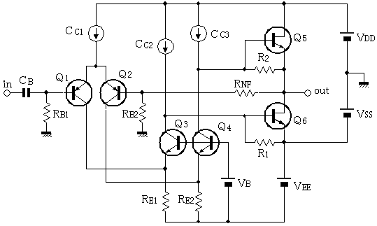
[Circuit 1] The simplest circuit
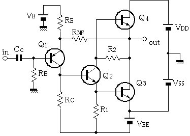
Idling current is Q 3 drain current I D3 determined by , Q 4 drain current I D4 , NFB is I by the action of keeping the midpoint voltage to 0V D3 equals.
I D3 change of , in this case Q 3 Apart from the temperature characteristics of, Q 3 power supply voltage V of the SS and Q 3 gate-to-source voltage V of the GS3 generated by a change in you.
I D3 variation of, [Delta] I D3 = [Delta] V SS / r D - [Delta] V GS3 · g m [r D : Q 3 drains of the internal resistance, g m : Q 3 transconductance]
g m = mu / r D So, [Delta] I D3 = ([Delta] V SS - [Delta] V GS3 · mu) / r D [mu: Q 3 voltage gain of]
If, delta = [Delta] V GS3 if · mu [Delta] I D3 is Occurs No.
If R1 = R2, then V GS3 = V EE / 2, so ΔV GS3・ μ = Δ ・ μ / 2.
Therefore, if the power supply is designed so that the relationship of V EE = 2V SS / μ can be maintained, this fluctuation factor of idling current can be eliminated .
To set the midpoint voltage to 0 V, Q 1 adjusts the bias voltage V E to cancel the base-emitter voltage V BE 1 so that V E = V BE 1 . Since V BE1 has temperature characteristics, V E must also have the same temperature characteristics as V BE 1 .
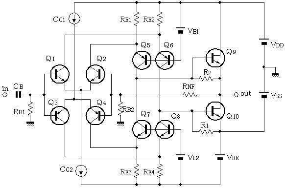
[Circuit 2] Constant current load (active load) method
When the load of Q 1 is set to the constant current circuit C C , the open loop gain becomes large and NFB is strongly applied, so low distortion and low output impedance can be achieved.
If C C has the same temperature characteristics as Q 1 , the midpoint voltage does not fluctuate due to temperature.
[Circuit 3] Differential amplification current mirror PP method
V E can be omitted by replacing the first stage with differential amplification . When the differential output is push-pull combined using a current mirror, the open loop gain becomes large and NFB is strongly applied, so that the distortion factor and output impedance can be lowered, as in the active load.
Q 1 and Q 2 Then , if the temperature characteristics of Q 3 and Q 4 are the same, the midpoint voltage does not fluctuate due to temperature.
I think this is one completed form.
A little concrete circuit
In Q6, pull up the voltage at the R2 end with reference to the source voltage in Q8. Adjust the voltage at the R2 end with VR1 (a fixed resistor is also acceptable).
D1 and D2 are devised to prevent the withstand voltage (100V) of CRD from being exceeded.
Adjust the idling current of Q8 and Q9 with VR2.
The power supply ground is connected via 100Ω so that it is safe even if an output point voltage offset occurs. 100Ω may be 1kΩ as long as the leakage current of the electrolytic capacitor is small.
[Circuit 4] Differential amplification folded cascode method (A)
In order to eliminate the variation of the idling current in this circuit, C C1 C to the constant C2 and C C3 , or C C2 and C C3 C with a constant C1 , and V SS will be changed in conjunction with the change of ..
[Circuit 5] Differential amplification folded cascode method (B)
To eliminate fluctuations in idling current in this circuit, keep C C1 , C C2 , and C C 3 constant and change V B in conjunction with the change in V SS .
[Circuit 6] Differential amplification folded cascode method (C)
To eliminate fluctuations in idling current in this circuit, change V B1 , V B2 , C C 2 to C C 1 or C C 1 , C C 2 , V B 1 to change V B 2 to V SS . It changes in conjunction.
Circuit plan 6
The circuit plan 5 was reworked to adopt a tracking bias method in which the bias voltage Vgs of the SIT is changed according to the fluctuation of the power supply voltage Vss to keep the SIT idling current constant.
It took a lot of time to calculate the constant, but now it is possible to change Vgs according to the fluctuation of Vss.
However, in actual cases, this circuit is not practical because Vgs is expected to fluctuate significantly with a slight temperature change in resistance. There is a possibility that it can be improved by increasing the Vee and increasing the emitter resistance (3 kΩ) of the folded cascode.
This is the circuit I thought about during the Bon holidays.
There is no point in pursuing only the ideal, so I aimed for a realistic one in order to embody the amplifier in both rabbits and corners.
That said, I didn't want to make the existing circuit just a rehash of the bland one, so I tried to incorporate some fresh ideas.
Is this an attractive circuit that makes you want to hear the sound?
I still don't know what will happen with the mochi I drew in the picture, but I will actually make it and fix any problems.
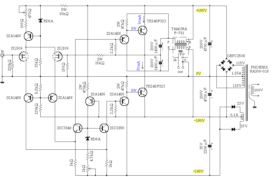
Circuit diagram No. 1 ( PDF size145kB)
The first circuit is a high gain amplifier that synthesizes the output of the cross shunt differential circuit by the current mirror push pull in the first stage.
The output is given to the emitter follower that drives the SEPP output stage by SIT, but the phase is inverted by the inverting amplifier with a gain of 1 to the upper side, and it is given directly from the point where the level is shifted by the Zener diode to the lower side. By doing this, it is possible to fully swing the upper SIT in the negative direction.
A PNP transistor is used for the emitter follower, and the gate-source voltage of the SIT can be swung up to + about 0.6V by the voltage drop between the base and emitter. In SIT, when the gate-source voltage becomes + 0.5V or more, the gate current flows out and the saturation voltage between the drain and source drops to about several V, so there is no need to apply a higher gate-source voltage. In addition, the voltage drop between the base and emitter is a negative temperature characteristic, so it also serves as SIT temperature compensation. Naturally, the low impedance drive can drive up to a high frequency against the mirror capacitance generated in the SIT, and I think this drive method is the best match for the SIT.
Since the source of the lower SIT is -160V, the power supply of the lower emitter follower is also based on -160V, but since the source of the upper SIT is the output of the SEPP circuit, the power supply of the upper emitter follower Must be a floating power source that operates on the output voltage from the output of the SEPP circuit. Therefore, in this circuit, the output side and the ground side are AC-isolated by the inductance of the output transformer, and DC current is supplied from the DC power supply at the ground base point to the bootstrap capacitor in the upper emitter follower to supply the bootstrap capacitor. The voltage stored in the capacitor is used as the power supply for the upper emitter follower. The bootstrap capacitor also works by blocking the DC component from the output point of SEPP and sending only the AC component to the output transformer (which is the main thing).
In order to reduce the fluctuation of the idling current when the power supply voltage of SIT changes, 1 / μ of the drain supply voltage is given between the gate and source in opposite phase. The mechanism is 5,6kΩ and 2kΩ in the base bias circuit of 2SA1191, and the voltage which rectified 28V of the power transformer is divided into about 1/3 and generated on the emitter side of 2SA1191. Since 28V of the power transformer is 1/4 of the SIT power supply 112V, 1/12 of the fluctuation of the SIT power supply voltage is generated on the emitter side of 2SA1191. And since 1/2 of the voltage fluctuation on the 2SA1191 emitter side is the change in the voltage between the gate and source of each of the upper and lower SITs, the fluctuation of the power supply voltage of SIT is 1/2 between the gate and source of SIT. Since / 24 is added and the μ of SIT is about 24, the idling current can be kept constant even if the power supply voltage fluctuates.
Circuit diagram No. 2 ( PDF size195kB)
In the second issue, the output of the first stage is transmitted to the SEPP side with a folded cascode. Since the gain of the first stage is low, the amount of feedback is small and the characteristics will be inferior to the first one, but since the signal path is simple, there is an expectation that the sound quality will be superior.
By connecting 2SJ109 of the cross shunt circuit and 2SJ109 of the pair to the emitter side of the folded cascode circuit with a constant current, the drift component due to 2SJ109 of the cross shunt circuit can be canceled. Therefore, in order to keep the voltage between the drain and source of both 2SJ109s always equal, the cascode bootstrap circuit is adopted for the cross shunt circuit.
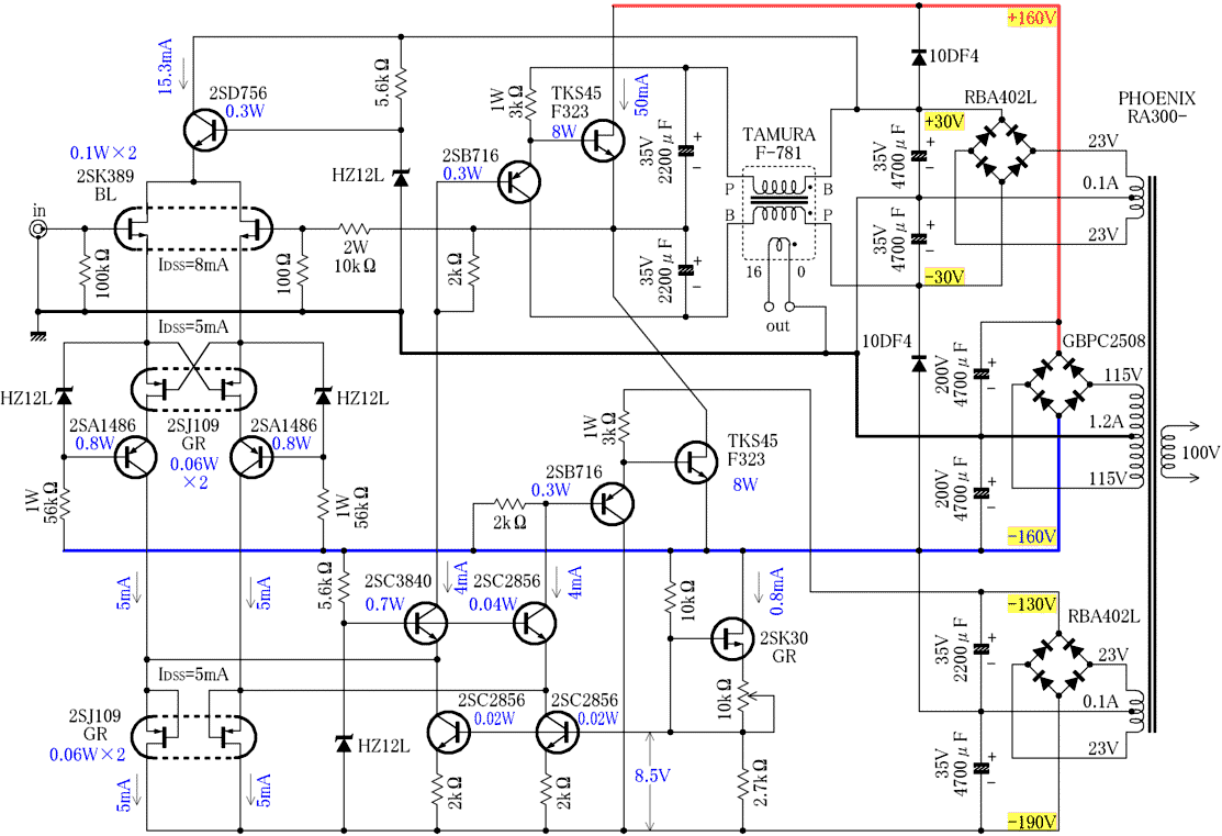
Experiment with SIT power amplifier circuits
Try Gatten Tracking Bias
The method of changing the bias voltage of the SIT according to the fluctuation of the power supply voltage is called tracking bias.
The experimental circuit is shown in the figure below.
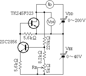
As the drain-source voltage V DS of the TKS45F323 rises , the drain current I D tends to increase due to the drain internal resistance r D of the TKS45F323, while the 2SC2856 negatively increases the gate-source voltage V GS of the TKS45F323. I increased D because it reduces the, V is in a state in which both of the action is to just balance DD I also changed the D should keep a constant value. Since the change ΔI D of I D is ΔI D = ΔV DS / r D -ΔV GS · μ / r D , the condition for ΔI D to be 0 is ΔV DS = ΔV GS · μ. Since the emitter resistance and collector resistance of 2SC2856 are equal at 5.6 kΩ, the gain is -1, so ΔV DS = ΔV GS ・
To a mu is the base side of 220Keiomega 2SC2856 / (R B are considered may be set + 8.2kΩ) to mu-1.
The μ of TKS45F323 is about 24 when V DS = 160V and I D = 50mA.
In order to see how it can be placed at the operating point of the amplifier , V EE is adjusted so that I D = 50mA at V DS = 160V, and the data obtained by changing V DS and measuring I D is shown in the figure below.
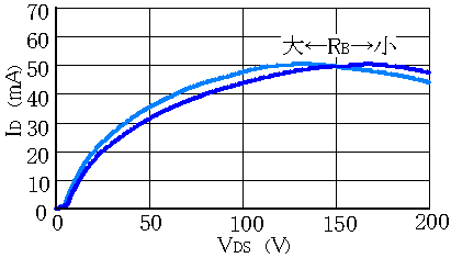
The change in I D with respect to V DS becomes a semi-cylindrical curve, and increasing R B moves the maximum point of I D to the lower side of V DS . V in the vicinity of the operating point DS in I D can be prevented large variations in, it is impossible for a predetermined reduction in a wide range. Reason for this is V DS is considered to be due to a decrease in μ in proportion to the rise of. If R B is set to a large value, ID will decrease when V DS becomes high, and the risk of excessive drain loss due to an increase in power supply voltage can be prevented.
Power drift cancel circuit
Since the tracking bias can make the idling current constant with respect to fluctuations in the power supply voltage, if the idling current can be made constant with respect to the ripple noise voltage of the power supply, operation that is not affected by the power supply noise becomes possible.
To do so, consider a circuit that detects the fluctuation of the drain power supply voltage of the SIT, inverts the phase, divides the voltage into 1 / μ, and applies it between the gate and source of the SIT.
With this power supply drift cancel circuit, the drain current does not change even if the drain power supply voltage fluctuates, so the drain internal resistance of the SIT becomes equivalently higher than the drain power supply.
On the other hand, the drain internal resistance of the original low SIT acts on the drain load, so I think that it is a circuit system that is perfect for SIT.
Eyes are ten temperature coefficient
Why do not you simply examine experimentally the temperature characteristics of TKS45F323, I is zero bias state D is negative temperature coefficient from more than about 0.2 A, I apply a negative bias when the temperature coefficient is negative D is larger point It turns out that it moves in the direction.
Therefore, since the temperature coefficient is positive at V DS = 160V I D = 50mA, which is the operating point of the amplifier, I D increases as the temperature rises .
The temperature coefficient with a negative SIT is a story in the low voltage and large current range, and in the case of small current and high voltage operation, there is a risk of thermal runaway unless temperature compensation is applied.
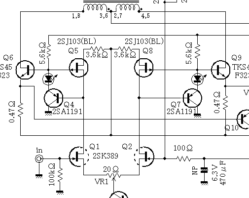
Experimental circuit part 1
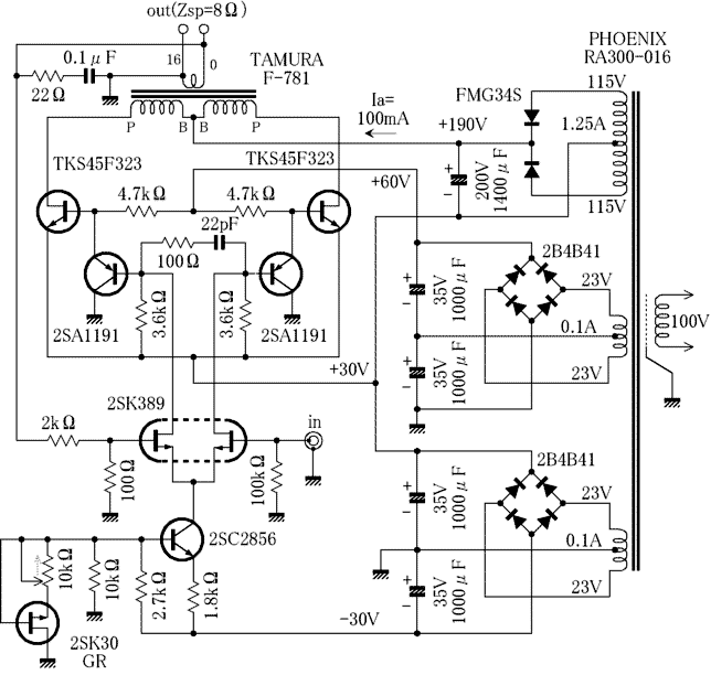
I tried to operate the double-end push-pull circuit shown above by barracks with the parts at hand.
The output starts clipping from about 20W, but since it is a soft clip, it can output up to nearly 30W.
The output impedance is 2.5Ω without feedback, and when NFB is applied from the secondary winding, it becomes about 0.6Ω. In addition, Tamura F-781 has an NF winding, so when NFB is applied from there, it is about 1.2Ω.
Since it oscillates when NFB is applied, 100Ω + 20pF is put in the load of the first stage differential amplifier, and the output is dumped at 22Ω + 0.1μF because it oscillates when there is no load. It's dirty.
The emitter follower drive with PNP transistors seems to have worked. If a silicon diode 1S1588 is inserted in series with the emitter of 2SA1191 and the voltage is raised by 0.6V, the output clip will be hard, but if the input voltage is increased further, bumps will occur in the clipped waveform and it will become ugly. I will.
The stability of the idling current was tested by making it easier for the temperature to rise with a small radiator plate in order to see the effect on temperature changes, but it is stable due to the effect of heat coupling the 2SA1191 on the TKS45F323 and compensating for the temperature. .. In addition, with respect to changes in the power supply voltage, it does not change significantly as the voltage increases, even if it rises slightly. The drain current at power- on becomes a large current (0.3Amax) in the section where the rising voltage is low ( peaks when V DS = 15V).
■ Since the ripple of the power supply is canceled by the push-pull operation, it does not occur in the output if the pair characteristics of SIT are aligned. Although it is a condition that it is within the class A operating range, ripple noise is worrisome when there is no signal or when the volume is low, so unless the idling current is extremely low, there will be no problem.
Ripple and power supply voltage fluctuations cause fluctuations in idling current, so tracking bias is necessary to prevent this.
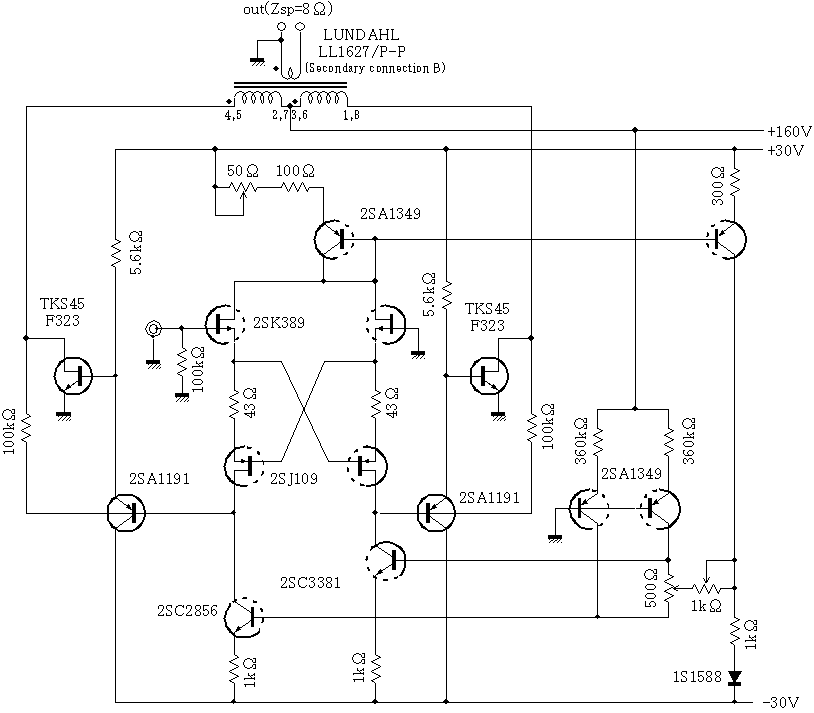
Modification of experimental circuit 1
Lundahl LL1627 / PP is adopted as an output transformer, and drain gate feedback is applied to SIT to lower the output impedance.
The power supply drift cancel circuit used in EL34 super triode connection Ver.1 has been incorporated.
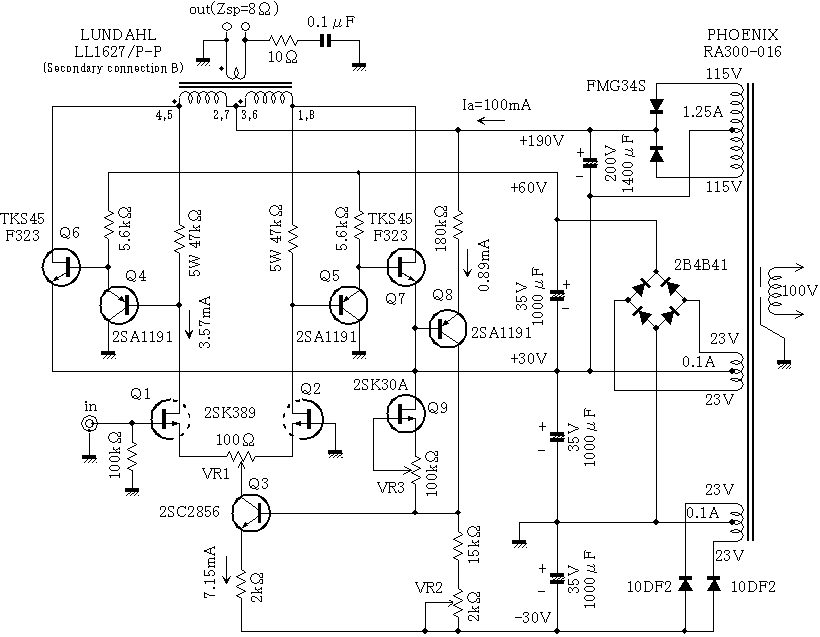
The four coils on the primary side of the output transformer Lundahl LL1627 / PP were used in two parallels and two series, and the eight coils on the secondary side were used in four parallels and two series.
The impedance ratio between the primary side and the secondary side is 538Ω on the primary side when the secondary side is 8Ω, calculated from the measured value of the voltage ratio.
The adjustment method is to set VR1 to the center, maximize VR2 and VR3, gradually raise the power supply voltage with the slidac, adjust VR3 so that the idling current Ia keeps 100mA, and raise or lower the power supply voltage with VR2. Adjust so that the idling current does not change.
VR1 is adjusted so that the output power supply ripple noise is minimized, and the residual noise is about 70 μV.
There is a problem with the stability of the idling current.
Since the temperature coefficient of 5W47kΩ (metal oxide film resistance) is large, the idling current will not be constant until this heat generation and heat dissipation are balanced.
A simple calculation shows that when the temperature coefficient of 5W 47kΩ is changed by 20 ° C at 100ppm (100 x 10 -6 / ° C), the resistance value changes by 94Ω and the gate voltage of SIT changes by 0.336V. If gm is 0.5S, the drain current will change by 168mA.
This circuit needs to be radically reviewed, as even a metal film resistor with a temperature coefficient of 25 ppm can only improve the variation by a quarter.
The circuit is incomplete, but the result of mounting and testing the output transformer is as follows.
The output in front of the clip is 60W, and because the clip is soft, it is rounded even at around 80W.
At 20Hz, the waveform begins to collapse from around 40W.
At 30Hz, the waveform does not collapse at either 60W or 80W.
The high range drops by -2.6dB at 100kHz.
The output impedance is 0.8Ω.
Frequency characteristic measurement data of output transformer Lundahl LL1627 / PP alone (primary side voltage Vp = 2.72V constant)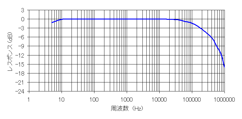
Revision of experimental circuit 1
I've tried various things, but in the end I ended up with a circuit like this.
Since it still oscillates under a capacitive load, countermeasures remain, but the residual noise has achieved 26 μV, which is a personal best.
It's strange that when you come to this point, you feel like you need to do this. As I recall, it was the same when I reduced the distortion factor, and when I widened the frequency response. Only then did I feel that I was able to know the characteristics of the amplifier I needed.
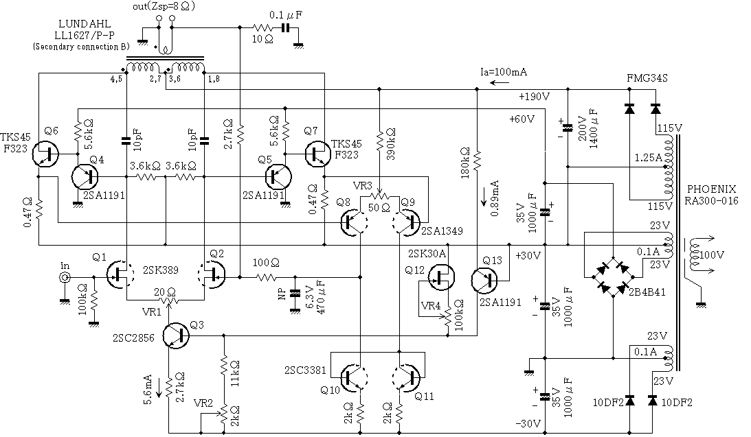
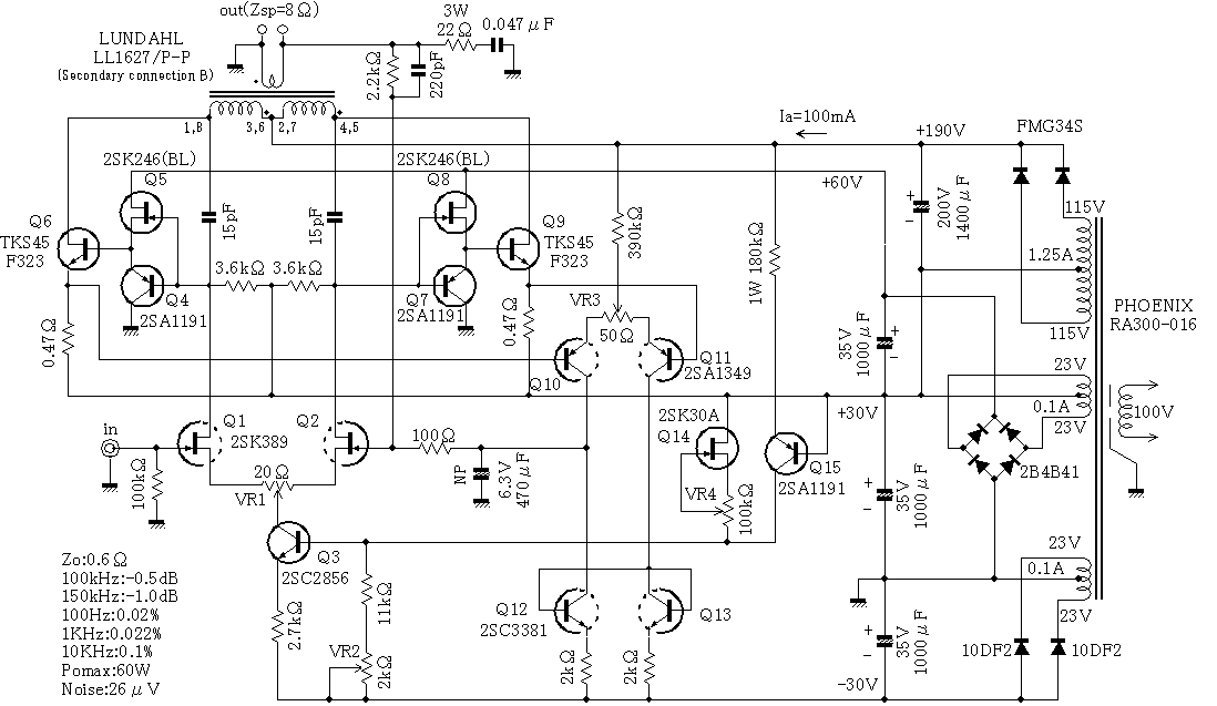
Experimental circuit No. 1 Kai Kai Kai
Push-pulling the SIT drive slightly improved stability under capacitive loading.
The performance is much better than this circuit example , but the circuit is complicated by that amount. However, the difference in sound will be small compared to that.
Despite this, the reason why I do this is because I heard the voice of SIT asking me to do this.
I am happy that I was able to meet that wish.
It's not a joke, I can't help but hear the voice that I'm screaming and screaming at the one-man sumo wrestling, but it's also fun to see that.
Barracks set during experiment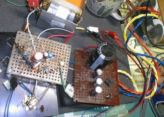
Other experiments that did not come to mind
I tried driving the SIT with a voltage mirror circuit, but I didn't like the clip waveform at the maximum output, so I didn't use it.
The SEPP circuit requires a radiator for the high withstand voltage transistor, and the circuit scale is not enough, but the quantity is also large.
If that improves the characteristics, I will put up with it, but I will lose motivation because it is like DEPP.
This circuit was the most miserable.
A cross shunt connection is used in the first stage, and the SIT source is set to the ground potential. Well, that's good, but I thought about putting a constant current circuit on the load side of the first stage and copying the current value of the constant current circuit with the current mirror on the upper side of the first stage. But that didn't work. This is because if no current flows through the constant current circuit, no current is generated on the upper side of the first stage. "Be aware before you do it!"
Kaneda style complete pair SIT-2SJ18 power amplifier
2008/09/00
SONY-2SJ18

In the meantime, the complete circuit was announced, and the 2SK60 circuit was announced in the September 1994 issue. The circuit of 2SJ18 was not announced, but it was made this time because it should be possible to drive with almost the same circuit.
Of course, I saw some people trying on the internet, so I used it as a reference.
The following table measures the variation of the obtained Tr. The measurement conditions are Vds = 22V and Vgd = 7.6V.
| 1 | 2 | 3 | 4 | 5 | 6 | 7 | 8 | 9 | 10 | |
| ID (mA) | 206 | 45 | 76 | 38 | 127 | 169 | 53 | 46 | 26 | 145 |
The rating of 2SJ18 was listed in the June 1975 issue, so I will post it as follows.
| item | symbol | conditions | minimum | standard | maximum | unit |
| Drain gate leakage current | Idgo | Vdg = -100V ・ Is = 0 | -0.1 | -100 | μA | |
| Gate cutoff current | Isgo | Vgs = -30V ・ Vds = 0V | -0.1 | -100 | μA | |
| On voltage | Von | Ig = -0.2A, Id = -3A, | -Ten | V | ||
| Cut-off voltage | Vp | Vds = -60V, Id = -100mA | 7.5 7.5 | 18 | twenty five | V |
| Input capacity | Ciss | Vgs = 15V, Vds = 0V, f = 1MHz | 190 | pF | ||
| Cutoff frequency | fT | Vds = -20V, Id = -0.5A | 20 | MHz | ||
| Voltage amplification factor | μ μ | Vds = -20V, Id = -1A, f = 1kHz | Four | |||
| Output resistance | rD | Vds = -20V, Id = -1A, f = 1kHz | 16 | Ω | ||
| item | symbol | |
| Voltage between gate and drain | Vdgo | -170V |
| Voltage between gate and source | Vsgo | -30V |
| Drain current | Id | 5A |
| Gate current | Ig | -0.5A |
| Allowable power loss | Pt | 63W |

I don't know whether to use the cut-off voltage or the on-voltage as a reference, but I thought about driving up to the cut-off voltage with a margin. Therefore, it is designed to increase the drive resistance and increase the voltage compared to MOS-FET.
Next, considering the power supply voltage of the voltage amplification stage on the + side, the positive side drive voltage of the 2SJ18 touches the + side from the power supply voltage of the output stage, so this voltage and the voltage of the cascode circuit of the 2SJ77 should be added to determine. However, it is estimated that at least 50V is required. The above circuit was designed with the above in mind, but it did not work with this circuit.
By the way, 2SJ18 needs to make the bias voltage deeper than the source voltage, so it is necessary to pay attention to the power-on timing. If the output stage rises faster than the voltage amplification stage, an excessive current will flow to the FET. With that said, power supply design must be more careful than ever. I think the main reason why I hadn't been able to make this device endlessly while getting this device was because I was worried about how to design the power supply.
Experimental power supply

The transformer is A-35S for Tango A class 15W. Since this transformer does not have a proper winding for the voltage amplification stage, I prepared a separate R core transformer for the voltage amplification stage. The voltage can be switched between 25V, 35V, 60V and 90V. The power amplifier can also be used for preamplifier experiments.
This time, the experimental power supply was partially modified to provide a delay circuit in the output stage. 2006/11 issue This is a port of the delay circuit of the vacuum tube type power amplifier as it is.
Protection circuit

In addition, since the wiring uses a universal board, it is changed instead of according to MJ. I attached two LEDs. This allows you to check the operating status of the counter. You don't have to be frustrated until it works.
Also, the article pattern still needed to be modified. One thing to be careful of is that some IC foot numbers are exactly the opposite. If you made a delay circuit and it didn't work out, you should check the direction of the IC again.
Amplifier board

Temporary assembly of only one channel

Oscillate at high frequency

Final circuit

At this time, there was no way to figure out what was going on, and it was feared that it would be completed. A couple of days later, when I was researching various things, I saw an example of an amplifier using 2SJ18 announced on the net, and noticed the difference from the circuit I made. It was that the connection point of the voltage amplification stage and the gate of 2SJ18 was opposite on the +-side. I changed to that circuit immediately and it worked.
In addition, the idling current hardly flows even if the gate voltage is lowered to about 8V. Therefore, as shown in the circuit diagram, it seems that the gate voltage of the bias should be seen at about 7V, so I think that it is okay to estimate the power supply voltage of the voltage amplification stage that was initially considered to be lower than at the time of design and lower it from + 50V. .. However, there is no problem with the planned voltage so far, so leave it as it is.
For the above reason, the bias voltage as high as 18V is not required for the 2SJ18, so I thought that it was not necessary to make a voltage drop with the gate resistor, so I changed the 3.9kΩ for the bias of the 2SJ18 to 2.7kΩ. In addition, it is a plan to reduce the impedance as much as possible to deal with the input capacitance of the FET. However, if it is lowered too much, the gain of the entire amplifier may decrease and the amount of feedback may decrease.
The source resistance of 2SK214 was also changed to make the current of 2SJ74 around 6.0mA.
In addition, the reason why the first stage cascode Tr was set to 2SC1399 is to consider the withstand voltage, but if the voltage is to be lowered, it seems that it is okay to use FET. Since the FET configuration is used except for the constant current circuit in the first stage, it seems that the sound of the FET will come alive.
If 2N5465 is used for the first stage constant current circuit, it will be a complete FET configuration, but I often hear that 2N5465 was made to cry by this FET because it was difficult to obtain. In fact, I also have a hard time, so I use a constant current circuit with Tr.
I have removed the source resistance 0.47Ω of 2SJ18. The idling current was set to about 200mA. After investigating various old MJs, I came to the conclusion that it is better to let this idling current flow. In addition, I took it off and watched the idling current for a while, but it seems that there is no dust that the current increases, probably because I used a spare radiator.
Output waveform

Complete

2013/07/06
I thought it was completed, but it was oscillating!

It was completed around 2008, but at that time it wasn't connected to the speakers yet to produce sound. Earlier this month, when I connected it to a speaker and input a square wave, it turned out to be oscillating. For this reason, I modified a part of the phase correction circuit to stop the oscillation. That circuit is this. First, 620Ω + 510PF was connected to the first stage, 10Ω + 0.1μF was connected to the output, and 10μF of bipolar electrolytic capacitor was connected to the power supply of the power stage.


 As shown on the left side of the board table, was there a junk box for the output of AUDYN-CAP film 0.1μF and 10Ω resistor as specified in the old days? I think that the skeleton, the power supply of the power stage was 10μF, the non-polar electrolytic capacitor of Nippon Chemi-Con that was not for audio, and the supplier was RS Online.
As shown on the right side of the board, 11pF of phase correction has been removed, and step type phase correction is 620Ω + 510pF directly attached to the back of the board. I started from around 1.2kΩ, but it didn't work. As far as the square wave response is seen with this value, it does not oscillate, so there seems to be no problem.
I started production more than 3 years ago, and finally I could hear the sound of SIT. However, it may not make sense to announce it because it is no longer available.


No comments:
Post a Comment