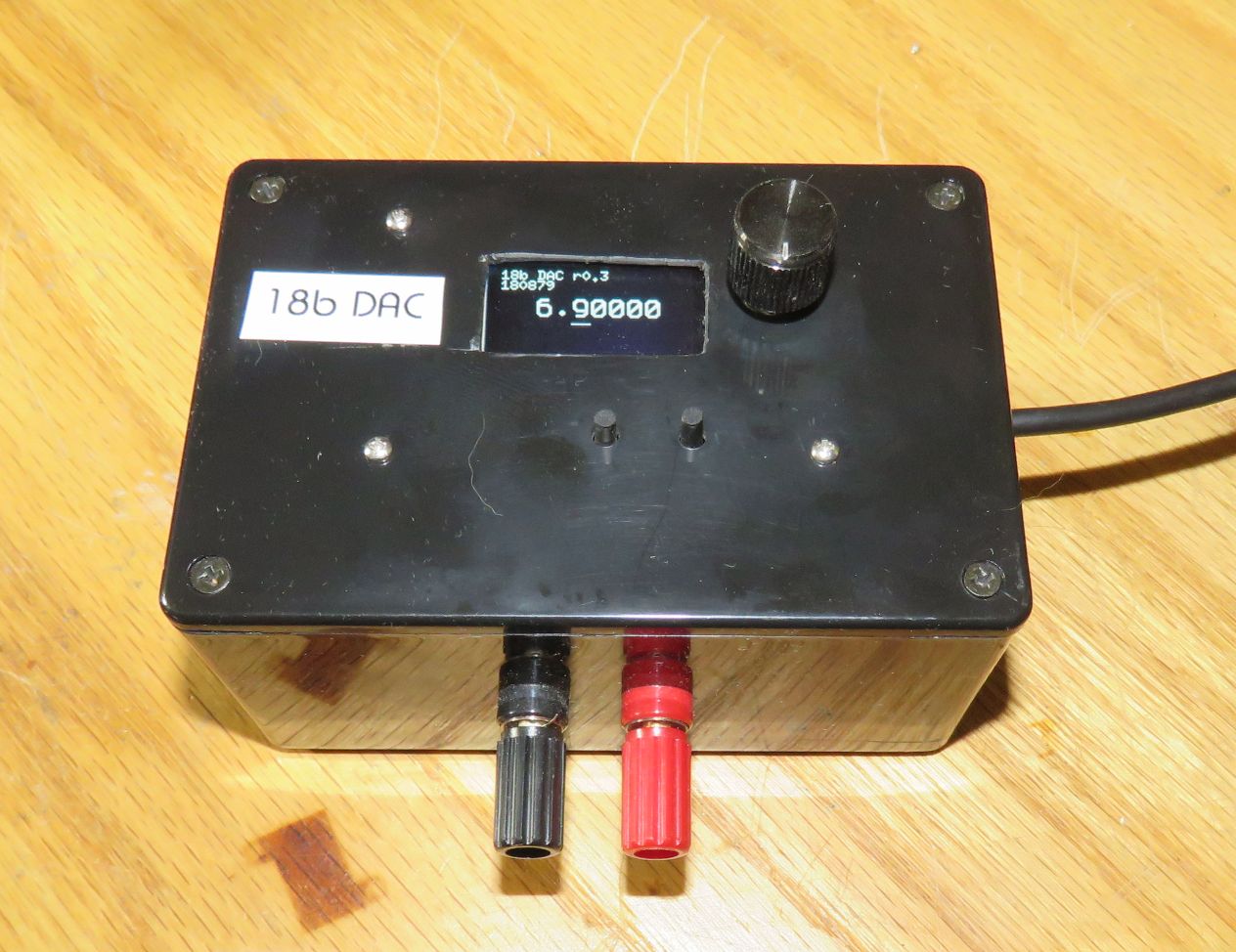
18 bit DAC: Precision Voltage Source
Introduction
我在Analogicg參與了AN8200精密20bit DAC的開發,這是非常精密的六位電壓源,輸出範圍可從100mV至最高1000V。
2000年代早期,這項產品是出自Data Precision唯一的產品線。為何?因為其具有驚人的表現且價格合理。因此,全世界的自動測試裝置系統通通採用了它。事實上它後來也被兩家以上的公司克隆。我想要建造一個相似的產品,但是更簡單、超便宜並更小。於是完美的選擇便是LTC275x 系列18 bit DAC。
這裝置應該有如下的能力:
It should have the following capabilities:
- 輸出範圍為0至5V以至正負10V
- 10ppm的精密度且飄移不超過10ppm
- USB或者前面板控制
- 全隔離
- 小巧且便宜:低於USD $100的零件成本
Design
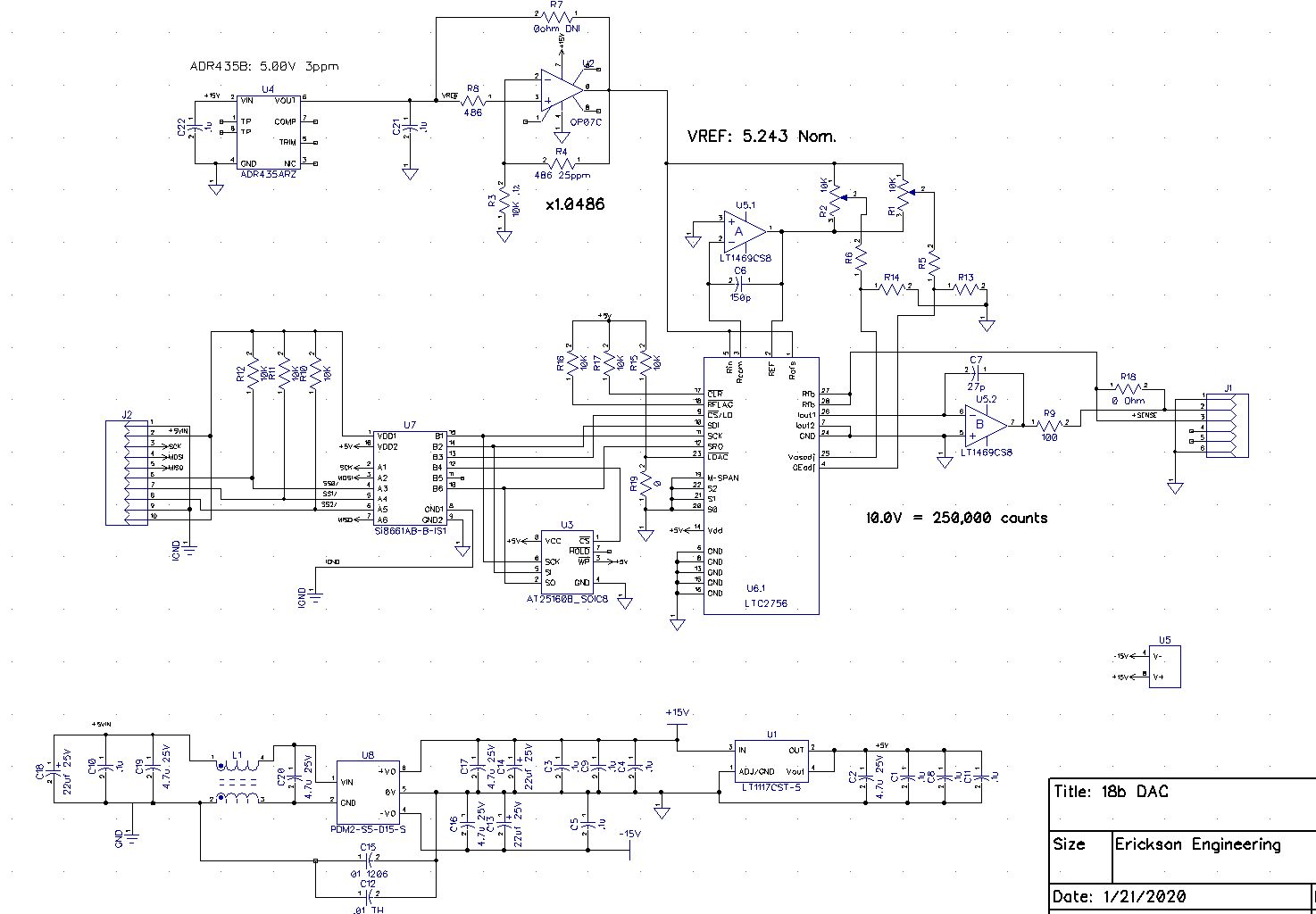
我很快地決定使用LTC2756A 單通道18BIT DAC,由於只打算製造少量的成品,因此會採用最好的A級。A級具有令人滿意的0.5LSB INL,售價USD 45元;而B級則是2LSB,35美元。以10V輸出來說,1 LSB代表40uV,0.5 LSB就是20uV,等效於10V的2ppm,相當棒!
Linear Tech的LT2756參考電路使用LT1468精密OP於電壓基準部分,以及作為輸出的I/V轉換器。我有一管的LT1469,也就是雙通道版本的LT1468,因此我決定採取雙通道設計;不過雙通道OP在精密線路中相較於單OP還是有一些輕微缺點。
- 雙OP功耗是單OP的兩倍
- 這代表兩倍的溫昇
- 以及約兩倍的偏壓飄移
- 以及更高的偏流以及飄移
- More complicated or compromised layout if the two circuits aren't naturally close.更複雜的線路或者犧牲最佳化佈線,如果線路原本就不夠接近的話。
- If one amplifier is the output amp, its temperature rise will increase with higher load current
- This can cause the reference section to drift with output load.
But.... the increased baseline power and therefore the temperature is fairly constant and so doesn't contribute too much to drift.
Also I think there generally will be a low load on this circuit, like micro amps. If I load it to much ( > 1mA) then I expect a bit more drift.
對於10V量程的設計,18BIT全用上的話就是262144步,但如果使用250000替代,則每步就是40.00uV,這會方便一點。
如果使用全18BIT,1 LSB就是38.147uV,就不方便了。於是我想到了一個簡單的解決方案。
Instead of a 5V reference, use 5.0 * 262144 / 250000 = 5.234V.
比起5V基準,使用5.0 * 262144 / 250000 = 5.234V為基準電壓。
額外好處是,量程稍微增加到10.486V;但是如何把增益調整為1.0486倍? 很簡單,採用non-inverting、低飄移的OP,並搭配溫度係數25ppm/0.1%的電阻。
為了得到一個放大1.0486倍的放大器,使用一個10.0K以及487歐姆的回授電阻即可。
因為10K以及487R僅貢獻5%的增益,因此每個25ppm的電阻僅貢獻25ppm的5%,僅為1.25ppm。
我在這一級採用了低成本的OP07。
For a 5V reference, I chose the ADR431 which is 3ppm/C.
To calibrate the output for near-perfect 0.0000V and 10.0000V, it is necessary to have gain and offset calibration.
Should I use a software cal or hardware trimpots?
With software you can't get much closer than about 1/2 LSB of offset error. And the gain calibration affects the DAC LSB step size.
And as long as the trimpots aren't contributing much change, they also don't contribute much signal change (or drift).
The LTC2756 DAC has convenient gain and offset adjust pins. Just feed in a low correction voltage to these pins.
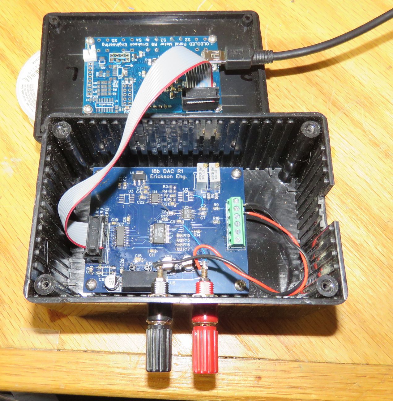
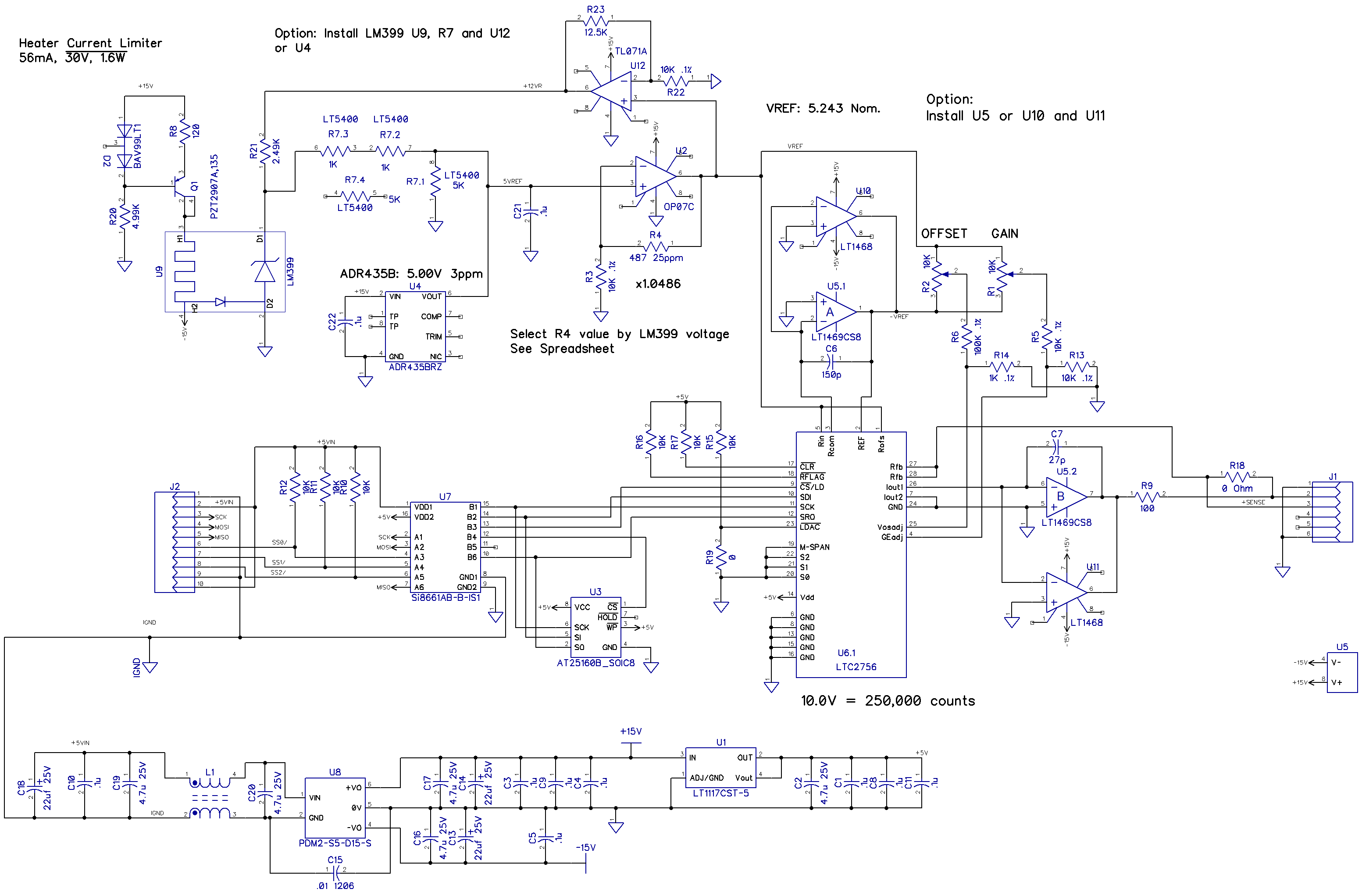
Here is the schematic diagram for Rev 1. J2 is the 5V power and SPI in connector, driven by LeoLed, my small front-panel Arduino board.
以下是內部照。
上面的板子是LeoLed的背面,LeoLed是一種搭載OLED顯示器的Arduino Leonardo控制器。
下面則是Rev0 18BIT DAC電路板。
控制Control
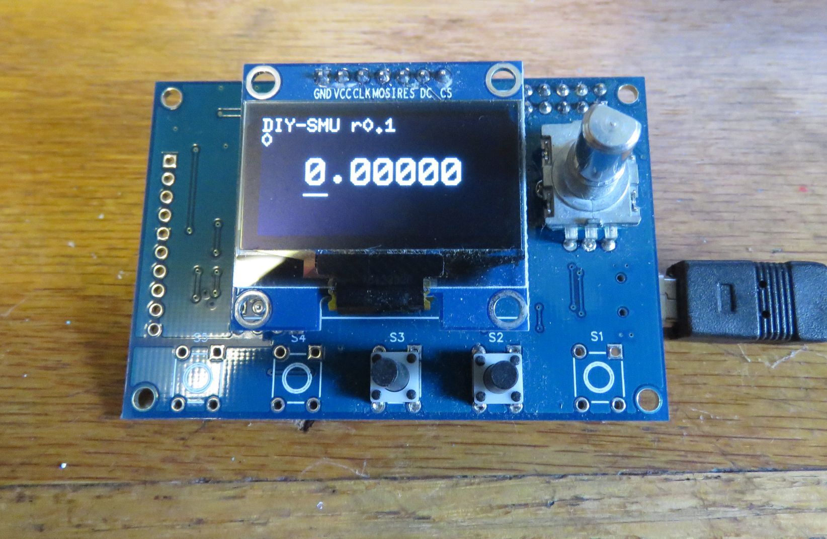
LeoLed搭載一個128X64的OLED圖像顯示器,另有Leonardo式的Arduino處理器。另外LeoLed也內建一個16位元的ADC以及優異的12位元DAC數個,雖然這個計畫用不到。
搭載14Pin的擴充端子具有+5V供電以及方便的IO。
可完美驅動精密SPI型DAC。
原本打算做為小型的量測面板以及控制器,不過我已經在數個計畫用上LeoLed,包含電子負載以及SMU。
LeoLed 特色:
- Arduino Leonardo (ATMEGA32U4) 處理器
- USB介面但不須 USB to serial轉換: faster USB, 不須設置Baud Rate
- +5V 供電自USB
- 128x64 1.3" OLED display, SPI
- Buttons for controls
- Rotary encoder with switch
- I2C 隔離器*
- 16b ADC, 12b DACs *
- 5V-5V隔離型DC-DC轉換器*
* 未使用於18b DAC 計畫。
For SPI data isolation. I like the Silicon Labs Si86xx series parts.
For this design the 6 channel part with 5 signals in one direction and one return signal will do: Si8661.
The power needs of this project are minimal.
A few tens of milliamps of +/- 15V, and +5V. A small 1 watt, +5V to +/-15V DC-DC provides the +/-15V as well as the required isolation.
A small +5V regulator makes the +5V.
It and the 18b DAC board mount nicely in a Hammond plastic box.
韌體Firmware
The firmware runs on an Arduino Leonardo-style (ATMEGA32U4) processor.
SPI graphics for the OLED使用U8G2 資料庫。
The hardware interface uses bit-bang SPI to drive the DAC.
I do this partially because the hardware SPI is busy doing the OLED graphics, and partially because the SPI requirements for this DAC are pretty slow.
對於低速SPI裝置,我通常只使用bit-bang SPI.
宣告SS/ pin low, set up a data bit (MOSI or SDI), and toggle the clock (SCK).
接著left-shift (data <<1) out however many bits are needed in a FOR loop.
For a READ, shift in the read data. It only takes a few instructions.
Depending on the slave, you need to control the clock polarity.
Analog Devices通常使用low-going clock.
LTC and TI 通常使用high-going clock.
以下是 bit-bang SPI 的常用方式,其方式為a 32 bit WRITE operation to the LTC2756.
/* Low-level Bit-bang 32 bit SPI Write for LTC2756 DAC.
Data is clocked in on + edge of CK\
Assert SS/, clock out 32 bits, de-assert /SS
*/
void spi32W(long data)
{
int i;
digitalWrite(SPI_CK, 0); // CK Should already be in this state
digitalWrite(SPI_MOSI, 0);
digitalWrite(SPI_SS, 1);
digitalWrite(SPI_SS, 0);
for (i = 0; i < 32; i++)
{
if (data & 0x80000000L) digitalWrite(SPI_MOSI, 1); // MOSI = 1
else digitalWrite(SPI_MOSI, 0); // MOSI = 0
digitalWrite(SPI_CK, 1); // Clock HI then LO
digitalWrite(SPI_CK, 0);
data = data << 1; // Shift up
}
digitalWrite(SPI_SS, 1);
}
The initial firmware uses an underline cursor to select the digit to be adjusted.
編碼器用來增減數值。
兩個按鈕控制游標的左右。
不巧的是,目前U8G2以及其他LCD顯示資料庫並沒有自動游標
因此我畫了一條短線位於合適的字元底下,並忽略了小數點,簡單有效。
關於更多韌體細節,參考 LeoLed digital panel meter。(失效!!!)
This project needs a proper USB control interface, so ATE tests can set the voltage and range.
此計畫需要合適的USB控制介面,以便於ATE測試可設定電壓及量程。
我計畫導入並測試Arduino SCPI資料庫,並參考DIY-SMU的程式碼。
如果有興趣,我會製造REV2電路板以除去一些需要跳線或者斷路的錯誤。
Ranges and Calibration量程以及校正
My plan is to use hardware only calibration on the 10V range.
This requires only multi-turn trimpots on the offset and gain trim pins.
So if you want the highest accuracy, use 10V range.
But hardware calibration takes, well, hardware, and is impractical to use on all the ranges.
I'm not sure how important the other ranges are.
The lower voltage ranges provide 1/2 the LSB voltage, so 20uV resolution.
The higher voltage ranges provide bipolar voltages such as +/- 10V and +/- 5V.
If you really need negative output, you could simply reverse the output terminals.
Negative output may be more important in an ATE environment.
As far as calibration of the other ranges, EEPROM corrections for offset and gain would need to be implemented. These would provide very good cal, +/- 1/2 LSB.
Rev2 計畫
Since I am looking at adding SCPI software control, I also am looking at a Rev2 PC board.
I originally built only one unit based on the Rev1 board.
It did not have the x 1.0486 amplifier so used 2^18 codes full scale for 10.00V.
But it worked very well, providing me with a very convenient, precision voltage to set the DIY-SMU project with.
I was having guilty second thoughts about my decision to use a dual op-amp.
It should be the builders decision, right?
So I made provisions for either a dual or two single op-amps.
Here are the changes for the Rev2 board.- Fix rework errors
- Op-Amp options
- Dual opamp (LT1469) or
- 2 singles (LT1468 or other)
- 5V reference options:
- ADR435: 3pppm / C
- LM399 + LT5400: < 1ppm / C, select-able R4 to correct for LM399 V
More Stable Reference Voltage: LM399
The Rev1 board had a few minor PCB errors that needed correcting.
And there was a bit of output voltage gain drift, traced back to the 5V voltage reference.
Particularly, ways to get better (1PPM) accuracy from these crude 7V +/- 3% devices.
For a perfect 5V, you can use an LT5400 matched resistor network which has < .5ppm tempco match.
They build a version with two 1K and two 5K resistors.
The two 1K's can be wired in series to get 2K. So it's ideal for building a 2K/5K divider for converting 7.0V to 5.0V.
But how to deal with the +/- 3% tolerance?
Turns out since 18bDAC wants a 5.243V reference to achieve 40uV / LSB,
adding a x1.0486 gain stage will do it, then just pick the value of R4 (shown as 486 ohms)
as a function of the LM399 voltage.
The gain will be nominally +4.86% (x1.0486), but can be easily adjusted from 1.000 to about 1.08 just by changing one resistor: R4.
It means you need to measure your LM399(s) first, then buy the correct resistor(s).
This is a preliminary schematic.
It has the latest changes including the heater current limit and the reference driver op-amp, but has not been built yet.
Wondering if I should add a +12V regulator.
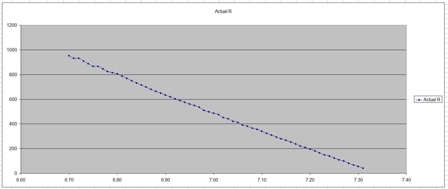
Since this stage only contributes 3-7% of the output voltage, it also only contributes 3-7% of the tempco drift. So a readily available 25ppm 0.1% resistor only contributes about 5% of 25ppm or 1.25ppm. Not bad for a $0.25 resistor. Here is a plot from a spreadsheet showing the R4 value to correct for a range of the LM399 Voltages. The bumps in the curve are because I use actual resistor values. The spreadsheet is in the project files above.
The LM399 heater draws significantly more power than the ADR435 reference. I measured about 1W, but the power draw peaks at about 2.5W during a cold-start of the LM399 heater. 2.5W is the maximum power to draw from a USB 5V connector: 5V at 0.5A. Would a USB C connector help? A solution is to add a current-limiting circuit to the LM399 heater. I can also use +/- 15V or 30V to power the heater, drawing equal and lower current from both +/- 15V supplies,
On my LM399 page I talk about some surplus (so free) precision resistor networks that I have. These have 12 resistors, two sets of 6. Each has 2x10K, 2x1K, 3340 and 3224ohms. It didn't occur to me at the time that I can put the two 10Ks in parallel to get 5K, and two 1Ks in series to get 2K. These are in a nice 16SOIC ceramic package, more convenient than the LT5400 in a SSOP-8 with heat tab. And free!
I have not yet ordered these PCBs. Copy this design at your own risk.
SCPI Control
For SCPI control,
I looked at 3 libraries I found:
Thanks to Vini from the OSMU project for the pointers.
One of OIC's examples implements a simple Source-Measure unit using Arduino ADC
and PWM pins: nice. I tested the code with various number formats for the voltage settings: Integer, fixed point, and scientific notation.
Now I'm changing the example to implement ranging, current measure, etc.
I tried all 3 libraries. Here is a quick review:
LachlanGunn/OIC
This one was easy to install and to run the examples.
I like that the basic example uses Arduino analog I/O.
I found it to be a bit touchy:
It seems to hang if you send it bad SCPI commands.
Interprets floating point numbers fine.
To specify commands is slightly cumbersome, requiring you to specify both the long and short forms as well as the string lengths.
source = scpi_register_command(ctx.command_tree, SCPI_CL_CHILD, "SOURCE", 6, "SOUR", 4, NULL);
scpi_register_command(source, SCPI_CL_CHILD, "VOLTAGE", 7, "VOLT", 4, set_voltage);
Vrekrer SCPI Parser
Also easy to install this library and run the basic example.
The basic example is a dimmer, and controls an LED brightness.
Command register format is more convenient.
Just call out the name once, and no need to specify string lengths.
Interprets Floating point fine. So far so good, I'll stick with this one for now.
BTW F("stuff") causes the string to live in Flash memory. I did not know that.
my_instrument.SetCommandTreeBase(F("SOURce"));
my_instrument.RegisterCommand(F(":VOLTage"), &SetVoltage);
my_instrument.RegisterCommand(F(":VOLTage?"), &GetSourceVoltage);
Jaybee.cz/scpi-parser
This one is not a native Arduino library.
It it quite large, about 10 .h files and another 8 .c files.
I spent a day trying unsuccessfully to coax it to compile on a Teensy, and then gave up.
A real programmer could probably do it.
I began with the OIC library.
I got it working on Teensy and on ATMEGA, and was happy with how quickly it came up.
18b DAC was crying for a proper way to control it via USB.
And unlike DIY-SMU, the 18b DAC is a simple project: Set the DAC to a voltage, done!
I moved the code to the LeoLed I use to control the 18b DAC.
The code fits, but is a tight squeeze on the ATMEGA32U4 processor.
Between the U8G2 library (with large fonts) and the SCPI Parser with floating point math,
it's up to about 23K of the 28K available flash memory.
For RAM, I use ~2K of the 2.5K available.
As long as I avoid too much feature-creep, it should be OK.
I'd like to implement SCPI on the E-Load project soon, as well as on the upcoming Switch (MUX) project.
Both of these projects use my LeoLed on a 'MEGA32U4.
The Vrekrer and OIC libraries are about the same size.
If I run short of RAM or Flash,
I could redesign LeoLed to use the newer
It does not have native USB like the 'MEGA32U4, but instead uses a small AVR processor as a USB to serial.
I haven't worked with this processor.
Another CPU upgrade option is
Teensy LC, a lower-cost ARM processor: 48MHz, 32b, ARM M0, 62K Flash, 8K RAM, lots of I/O, $12.
For the basic set of SCPI commands on 18b DAC, I use the following:
/*
* *IDN? -> identify
* *RST -> Reset to known idle state: 10V range, 0.00V
* :SOURce
* :VOLTage -> set_voltage
* :OUTput: -> <OFF/ON> (does nothing for now)
* :VOLTage? -> get_source_voltage
* :MEASure
* :VOLTage? -> get_voltage from an 10b ADC channel
*/
The :MEASure:VOLTage? command reads the Arduino 10b ADC.
It's just there to test some other SCPI commands.
I am happy that both parsers deal with all kinds of
number formats: 3, 3.14159, 3141.59e-3 all work fine.
Last Updated: 7/18/2021