VFET JFET Pre/Power Amplifier Circuits


The gain is 2.1 times.

Although it is missing in this circuit diagram, there is actually a 47u electrolytic capacitor between the power supply and ground.

Line input 0.5Vrms and output 1Vrms.

At this time, the VT62 full-stage differential amplifier in the latter stage reaches the maximum output, but such an output has never been output from the speaker.

I can't put it out in my environment.

I think I usually listen at a few milliwatts to a few tens of milliwatts.

Therefore, when proceeding to the case set in the future, I am thinking of biting an attenuator about 0.15 times the output of the flat amplifier.

Of course, I will make it a switching SW type and add 1x and mute.


Discrete Power OP-Amp


2SK79 VFET SIT V-FET Amplifier


SONY 2SK79 Small-Signal V-FET, TO-92 (S-D-G)
The rare Triode-like characteristics transistor made by SONY in 1970's, could be seen as a solid-state version of 12AX7 without filaments!
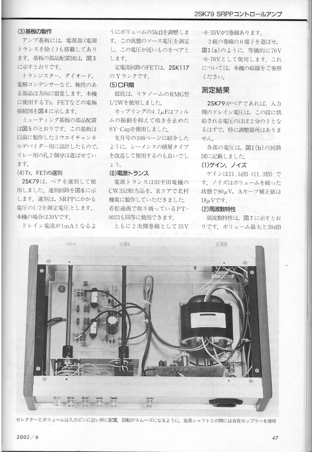
Vdg = 120V
Vsg = 10V
Id = 200mA
P = 750mW
rd = 2kΩ (Vds = 50V, Id = 4mA)
μ = 30 (Vds = 50V, Id = 4mA)
gm = 14mS (Vds = 50V, Id = 4mA)
Cip = 16pF (Vds = 50V, Id = 4mA)


2SK79 SRPP Non-Feedback PreAmplifier designed by Akira Yasui


Publication:
(1)
V-FET 2SK79 SRPP Non-feedback 1-stage amplification control amplifier
Author (1): Akira Yasui (安井 章)
 

(2) 
安井章,
MJ Radio and Experiment (Audio Technology MJ)
roll: 83  issue: Four  page: 142-150  Publication year: April 1996
JST document number: F0208A  ISSN: 1345-8817  Material type: Serials (A)
Country of issue: Japan (JPN)  language: Japanese (JA)


(3)
MJ無線と実験 2016年 09 月号 (Japanese) 
Print Magazine – August 10, 2016


MJ-Radio and Experiment, June 2002
2002/6 MJ RADIO


R5//RV1=200R


V-FET Driver 
2SK79 as input stage, 2SK60 and 2SJ49 as output stage.


Spice Models of 2SK79 VFET V-FET 

For SPICE Simulation, here are some SPICE models of 2SK79 in diff formats (LTSPICE, PSPICE, etc.)


/Model A/
* Created on 06/29/2020 09:20 using paint_kit.jar 3.1 
* www.dmitrynizh.com/tubeparams_image.htm
* Plate Curves image file: 
* Data source link: 
*----------------------------------------------------------------------------------
.SUBCKT 2SK79 1 2 3 ; Plate Grid Cathode
+ PARAMS: CCG=3P  CGP=15P CCP=1.9P RGI=600
+ MU=30.24 KG1=45 KP=106 KVB=337.5 VCT=0.0085 EX=1.54 
* Vp_MAX=93 Ip_MAX=10 Vg_step=0.2 Vg_start=0 Vg_count=10
* Rp=2720 Vg_ac=35.48 P_max=0.5625 Vg_qui=-0.9 Vp_qui=20.25
* X_MIN=163 Y_MIN=164 X_SIZE=1080 Y_SIZE=582 FSZ_X=1936 FSZ_Y=1056 XYGrid=true
* showLoadLine=y showIp=y isDHT=n isPP=n isAsymPP=n showDissipLimit=y 
* showIg1=y gridLevel2=n isInputSnapped=y  
* XYProjections=n harmonicPlot=y dissipPlot=n 
*----------------------------------------------------------------------------------
E1 7 0 VALUE={V(1,3)/KP*log10(1+EXP(KP*(1/MU+(VCT+V(2,3))/SQRT(KVB+V(1,3)*V(1,3)))))} 
RE1 7 0 1G  ; TO AVOID FLOATING NODES
G1 1 3 VALUE={(PWR(V(7),EX)+PWRS(V(7),EX))/KG1} 
RCP 1 3 1G   ; TO AVOID FLOATING NODES
C1 2 3 {CCG} ; CATHODE-GRID 
C2 2 1 {CGP} ; GRID=PLATE 
C3 1 3 {CCP} ; CATHODE-PLATE 
D3 5 3 DX ; POSITIVE GRID CURRENT 
R1 2 5 {RGI} ; POSITIVE GRID CURRENT 
.MODEL DX D(IS=1N RS=1 CJO=10PF TT=1N) 
.ENDS 


/Model B/

.SUBCKT 2SK79 1 2 3 ; Plate Grid Cathode
+ PARAMS: CCG=3P  CGP=15P CCP=1.9P RGI=600
+ MU=30.24 KG1=45 KP=106 KVB=337.5 VCT=0.0085 EX=1.54 
* Vp_MAX=93 Ip_MAX=10 Vg_step=0.2 Vg_start=0 Vg_count=10
* Rp=2720 Vg_ac=35.48 P_max=0.5625 Vg_qui=-0.9 Vp_qui=20.25
* X_MIN=163 Y_MIN=164 X_SIZE=1080 Y_SIZE=582 FSZ_X=1936 FSZ_Y=1056 XYGrid=true
* showLoadLine=y showIp=y isDHT=n isPP=n isAsymPP=n showDissipLimit=y 
* showIg1=y gridLevel2=n isInputSnapped=y  
* XYProjections=n harmonicPlot=y dissipPlot=n 
*----------------------------------------------------------------------------------
E1 7 0 VALUE={V(1,3)/KP*log10(1+EXP(KP*(1/MU+(VCT+V(2,3))/SQRT(KVB+V(1,3)*V(1,3)))))} 
RE1 7 0 1G  ; TO AVOID FLOATING NODES
G1 1 3 VALUE={(PWR(V(7),EX)+PWRS(V(7),EX))/KG1} 
RCP 1 3 1G   ; TO AVOID FLOATING NODES
C1 2 3 {CCG} ; CATHODE-GRID 
C2 2 1 {CGP} ; GRID=PLATE 
C3 1 3 {CCP} ; CATHODE-PLATE 
D3 5 3 DX ; POSITIVE GRID CURRENT 
R1 2 5 {RGI} ; POSITIVE GRID CURRENT 
.MODEL DX D(IS=1N RS=1 CJO=10PF TT=1N) 
.ENDS


Other Power VFET P-SPICE Models


*2SJ28
*GENERATED BY SIT MODELER @ AUDIOMAKER.TECH 
*MODEL RANGE: -55V, -5A 
*-------------------------------------------------- 
.SUBCKT 2SJ28 D G S ; Drain Gate Source 
+ PARAMS: MU=7.3 X=1.51 K=0.157 N=2.24 VCT=0 RG=2MEG 
*-------------------------------------------------- 
B1 D S I=-1*(K*PWR(URAMP((-V(G,S)+VCT)+(N*LN(-V(D,S))+(-V(D,S)/MU))),X)) 
*FOR LTSPICE
R1 G S {RG} 
CGS G S 0P 
CGD G D 0P 
CDS G S 0P 
.ENDS 2SJ28 
*--------------------------------------------------


** 2SK82 KD-33
*M. ROTHACHER
*--------------------------------------------------
.SUBCKT 2SK82  1 2 3 ; Drain Gate Source
+ PARAMS: MU=4.9140 EX=2.352 KG1=101.25 KP=75.0 KVB=24.0 VCT=7.04 RGI=2MEG
*--------------------------------------------------
E1 7 0 VALUE={V(1,3)/KP*LN(1+EXP(KP*(1/MU+(VCT+V(2,3))/SQRT(KVB+V(1,3)*V(1,3)))))}
RE1 7 0 1G
G1 1 3 VALUE={(PWR(V(7),EX)+PWRS(V(7),EX))/KG1}
RDS 1 3 1G   ; TO AVOID FLOATING NODES
D1 5 2 DX ; FOR GRID CURRENT
R1 5 3 {RGI} ; POSITIVE GRID CURRENT 
.MODEL DX D(IS=1N RS=1 CJO=10PF TT=1N)
.ENDS


VFET SIT V-FET POWER AMP

Brief  Parametric Table  of V-FET, SIT.

From small to large power V-FET.

2SK63 =~2SK79, 120V and Id=0.2A.


Pass SIT-1 by SemiSouth


TKS45F323 by TOKIN


2SK82 V-FET DC Power Amplifier


Hitachi LO-D HA-500F V-FET Power Amplifier, with V-FET 2SK89 and 2SJ29.


2SK70 V-FET Power Amplifier with CCS=0.8A


2SK82 Power Amplifier 
Nelson Pass, Single-Ended with output capacitor.


SONY Power Amplifer?


Yamaha B-1 Power Amplifier

B-1 or B-1 related ? Unsure.


Other Power VFET P-SPICE Models


*2SJ28
*GENERATED BY SIT MODELER @ AUDIOMAKER.TECH 
*MODEL RANGE: -55V, -5A 
*-------------------------------------------------- 
.SUBCKT 2SJ28 D G S ; Drain Gate Source 
+ PARAMS: MU=7.3 X=1.51 K=0.157 N=2.24 VCT=0 RG=2MEG 
*-------------------------------------------------- 
B1 D S I=-1*(K*PWR(URAMP((-V(G,S)+VCT)+(N*LN(-V(D,S))+(-V(D,S)/MU))),X)) 
*FOR LTSPICE
R1 G S {RG} 
CGS G S 0P 
CGD G D 0P 
CDS G S 0P 
.ENDS 2SJ28 
*--------------------------------------------------


** 2SK82 KD-33
*M. ROTHACHER
*--------------------------------------------------
.SUBCKT 2SK82  1 2 3 ; Drain Gate Source
+ PARAMS: MU=4.9140 EX=2.352 KG1=101.25 KP=75.0 KVB=24.0 VCT=7.04 RGI=2MEG
*--------------------------------------------------
E1 7 0 VALUE={V(1,3)/KP*LN(1+EXP(KP*(1/MU+(VCT+V(2,3))/SQRT(KVB+V(1,3)*V(1,3)))))}
RE1 7 0 1G
G1 1 3 VALUE={(PWR(V(7),EX)+PWRS(V(7),EX))/KG1}
RDS 1 3 1G   ; TO AVOID FLOATING NODES
D1 5 2 DX ; FOR GRID CURRENT
R1 5 3 {RGI} ; POSITIVE GRID CURRENT 
.MODEL DX D(IS=1N RS=1 CJO=10PF TT=1N)
.ENDS


V-FET Power Amplifier with 2SK70 and 2SJ20 complimentary stage, by Jean Hiraga in 1970's.
Jean Hiraga (l’Audiophile No. 11)
Class A, 60 Watts


The improved schematic can be modified so that it operates from Class A to AB. Simply, the modification relates to the 12 kohm resistors, which are replaced by higher resistances. 
Thus, the rated output power could be doubled, 
while increased power supply rail voltages are needed though.


However, in the case of using speakers with a relatively good output (as realised by Y. Neveu and J Mahul) the amplifier as described is sufficient in many systems intended for reproduction in an apartment, the noise level it makes can be very high.


However, the diagram can evolve with regard to the power. The basic circuit is not called into question, the changes relate to the power supply, the heatsinks and the transistors. 

The technology of the vertical field effect semiconductors, or power V-FET, makes it possible to obtain nearly 60 W under pure class A. 


Obtaining higher power passes naturally to the choice of other power transistors, such as V-FET, R.E.T. (Ring Emitter Transistor), MOS-FET, VMOS-FET, and Bipolar. 

It is necessary to note that the paralleling of output stages is not possible if the preceding stage does not have itself a parallel structure. 

Indeed, in the particular layout of the output stage, reversed Darlington, the driver transistor and the output transistor do not constitute, from a functional point of view, that of a single transistor.

 However, an output stage consisting of paralleled power transistors limits the performances as regards band-width and distortion, compared to a stage consisting only of a suitably selected single transistor with a higher Pc. 

In all the cases, the increased output power is accompanied by increased capacitance Cob, which is already sufficiently enough to limit the performance.


This can appear to be in contradiction with many " commercial " circuits. It should well be seen that at the mass production level, economic considerations are necessarily taken into account. 

In the catalogues of the American manufacturers in particular, there are transistors of very high power, with a Pc of more than 350 W, available in complementary pairs. 

In spite of this, in the construction of high power amplifiers, one prefers to employ the parallel layouts of transistors at a much lower cost price. The manufacturers can say what they want, but the perfect complementary pairs do not exist yet, in power transistors particularly. 

The use of a parallel arrangement inevitably results in placing the power transistors on various points of the heatsink. Also, the slightest variations in temperature immediately disperse the pairs, and inevitably disturb the operation of the amplifier. This is why we wait before publishing the description of an amplifier with high power and high quality. 

The progress of solid state physics and of semiconductors in particular, is so fast that we are persuaded that within one year, one will be able to find in the power MOS-FET and VMOS-FET series, transistors such that it will be possible to design a 100 W class A amplifier using only four transistors in all.

Because let us not forget that simplicity is a decisive criterion. 
At which time the prepreamp/preamp/amp unit uses only five or six stages in total?


Class A-Like Topology

- "New Class A" bias module (see Technics folklore - synchro bias) - "Super-A" bias module (see JVC folklore) - "No...